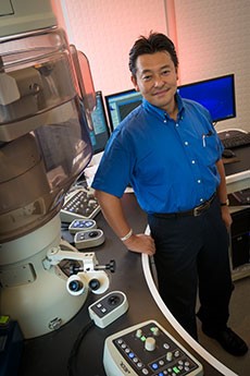
 When a single atom can make or break the successful development of new materials, it's the sensitivity of the microscope used that makes all the difference to researchers in materials science.
"You can't do research for tomorrow's materials by using yesterday’s microscopes," Asst. Professor Masashi Watanabe, Dept. of Materials Science & Engineering at Lehigh University says with characteristic humor.
Like many leaders in this field, Watanabe is influential in the development of the sophisticated instrumentation in his lab. Less than two years ago he installed what he calls "tomorrow's microscope in its current condition." The University has "the only Atomic Resolution Microscope with advanced aberration corrector and ultrahigh resolution pole piece in the Americas -- we can honestly say it's the best 200 kV microscope in the world."
With the installation of a 4th order ASCOR corrector, the Lehigh microscopy group is fully using the true potential of the ARM200F microscope.
Students and post docs at Lehigh examine the atomic structures in grain boundaries, or the interface between two grains or crystallites in metals. They also characterize ceramics and catalysis nanoparticles with the ARM.
"The ultimate goal is to find that one single atom in a bulk material, which could sometimes be an initial trigger to cause catastrophic problems if it locates at certain places such as the grain boundary. So, we try to find out which atom is responsible for the problem and then how many of them are causing it. Which means we have to quantify - we're not only seeing those different types of atoms, but also we quantify how many are there," he says.
Once they use the aberration-corrected STEM to find the atoms and X-ray analysis to determine the quantity of those atoms, they can modify the materials by eliminating those elements, modifying their sites, or creating a different kind of environment inside the materials.

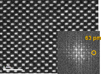
A HAADF-STEM image of [211]-projected GaN taken at 200 kV, with its FFT diffractogram.
Seeing atoms this clearly and with such stability opens new opportunities for the lab. Back in 2004 they installed an earlier high resolution microscope - the first JEOL aberration-corrected STEM in the U.S. - but now with the new ARM, which is more robust against environments; atoms can be observed with greater stability and improved resolution. The basement lab is outfitted with cooling and acoustic panels. The only concern is the skateboarders who jump on the concrete patio overhead - they are quickly asked to go elsewhere!
Dr. Watanabe has a very busy schedule as an associate professor, an organizer of symposiums for Materials Research Society and M&M, and now the President of the Microanalysis Society (MAS). He is principal author of the paper Improvement of Imaging Performance with a New ASCOR Probe-Corrector in a 200 kV JEM-ARM200CF published in Microscopy & Microanalysis in July 2016.
Even his undergraduate students get excited about materials science when they can see images taken by the ARM200F when he introduces a new concept such as the arrangement of grain boundary atoms.
Profile of Professor Watanabe