-
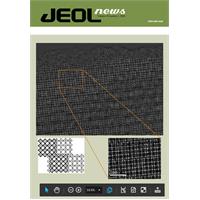
 Vol. 39 No. 2, 2004
• TEM Study of Water in Carbon Nanotubes
• A Study of Metal Nanowire Structures by High-Resolution Transmission Electron Microscopy
• Introduction of JWS-2000 Review SEM
• Grazing-Exit Electron Probe Microanalysis (GE-EPMA)
• Fullerenes and Carbon Nanotubes: Nanocarbon Assuming a Leading Role in the 21st Century
• Introduction of Products
-
 Vol. 39 No. 1, 2004
• A Double Aberration Corrected, Energy Filtered HREM/STEM
• Variable Magnification of Electron Holography for Junction Profiling of Semiconductor Devices with Dual Lens System on JEOL JEM-2010F
• The Electron Backscatter Diffraction Technique – A Powerful Tool to Study Microstructures by SEM
• Growth and Encystment of the Ciliate Tetrahymena sp. Found in a Dead Mosquito's Larva
• ALCHEMI Studies on Quasicrystals
• Electron Spin Resonance Spectroscopy in Food Radiation Research
• Cross Section Specimen Preparation Device Using Argon Ion Beam for SEM
• Introduction of new products
-
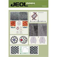 Vol. 38 No. 2, 2003
• Atomic Resolved HAADF-STEM for Composition Analysis
• Atomic Structure Analysis
• Direct Imaging of a Local Thermal Vibration Anomaly Through In-situ High-temperature ADF-STEM
• Cold-spray Ionization Mass Spectrometric Observation of Biomolecules in Solution
• Electron Spin Resonance (ESR) in Nanocarbon Research
• Analysis of Cadmium (Cd) in Plastic Using X-ray Fluorescence Spectroscopy
• JWS-3000 High-Resolution Review SEM
• Application and Extension of Pickup Method to Various Materials
• Introduction of New Products
-
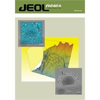 Vol. 38 No. 1, 2003
• Mapping of sp2/sp3 in DLC Thin Film by Signal Processed ESI series Energy Loss Image
• Electron Holographic Analysis of Nanostructured Gold Catalyst
• Single Atomic Column Observation in Silicon Boundary
• The Scanning Electron Microscope as a Tool for Experimental Nanomechanics
• Observation of Dislocation Structure of Fatigued Metallic Materials by Scanning Electron Microscopy
• Protein NMR - Ability of the JNM-ECA series
• Development of the JBX-3030MV Mask Making E-Beam Lithography System
• Chromatic and Spherical Aberration Correction in the LSI Inspection Scanning Electron Microscope
• Peak Deconvolution Analysis in Auger Electron Spectroscopy II
• Applications of Micro-Area Analysis Used by JPS-9200 X-ray Photoelectron Spectrometer
• Introduction of New Products
-
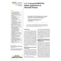 Vol. 37 No. 1, July 2002
• A Cs Corrected HRTEM: Initial Applications in Materials Science
• Quantitative Environmental Cell - Transmission Electron Microscopy: Studies of Microbial Cr(VI) and Fe(III) Reduction
• Simulations of Kikuchi Patterns and Comparison with Experimental Patterns
• Experimental Atomically Resolved HAADF-STEM Imaging - A Parametric Study
• Observation of Waterborne Protozoan Oocysts Using a Low-Vacuum SEM
• A Possible Efficient Assay: Low-Vacuum SEM Freeze Drying and Its Application for Assaying Bacillus thuringiensis Formulations Quality
• Observations of Algae and Their Floc in Water Using Low-Vacuum SEM and EDS
• Development of Nano-Analysis Electron Microscope JEM-2500SE
• Development of JSM-7400F
• New Secondary Electron Detection Systems Permit Observation of Non-Conductive Materials
• Applications of Image Processing Technology in Electron Probe Microanalyzer
• Technology of Measuring Contact Holes Using Electric Charge in a Specimen
• Organic EL Display Production Systems - ELVESS Series
• In-Situ Observation of Freeze Fractured Red Blood Cell with High-Vacuum Low-Temperature Atomic Force Microscope
• Peak Deconvolution of Analysis in Auger Electron Spectroscopy
• JEOL's Challenge to Nanotechnology
• Progress in Development of High-Density Reactive Ion Plating
• Applications of High-Power Built-in Plasma Gun
• Introduction of New Products
-
 Vol. 35 No. 1, July 2000
• 100kV E-Beam Lithography System: JBX-9300FS
• Gate Oxide Characterization using Annualr Dark Field Imaging
• JEOL Intro of New Products
• Kankan Diamonds (Guinea): probing the lower mantle
-
 Vol. 34 No. 1, July 1999
A 1000kV TEM Running Over 25 Years
• Atomic Resolution Z-Contrast Imaging of Interfaces and Defects
• The Growing Role of Electron Crystallography in Structural Biology
• Factors Promoting R&D in Electron Microscopy in Japan
• The Development and Assessment of a High Performance FE Gun Analytical HREM for Materials Science Applications
• Immunogold-labeling in Scanning Electron Microscopy
• Measure Contact Potential Difference Using an Ultrahigh Vacuum Noncontact Atomic Force Microscope
• Microscopic Chemical State Analysis by FE-SAM with Hemispherical Energy Analyzer
• Miniaturized STM Working Simultaneously in UHV Electron Microscope
• High-Resolution Electron-Beam Lithography and Its Application toMOS Devices
• Development of Optical Technology for JEOL's Electron Probe Instruments
• Observation of Protein Structures through an Electron Beam
• Transition of JEOL's Semiconductor Equipment, and Future Development
• Applicatrion of Semi-in-Lens FESEM for Chargeless Observation
• Development History of JEOL's Transmission Electron Microscopes
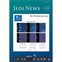 Vol. 54 No. 1, July 2019
• Atomic-Resolution Imaging and Spectroscopy on Materials of Various Dimensions by Aberration-Corrected Scanning Transmission Electron Microscopy
• Probe Corrected STEM Structural Imaging and Chemical Analysis of Materials at Atomic Resolution
• Analytical SEM and TEM: Applications in Product-related Material Development
• Practical Solutions in Electron Beam Lithography with the JBX-9500FS and the JBX-6300FS
• Development of New Operando Measurement System by Combining Reaction-Science High-Voltage Electron Microscopy and Quadrupole Mass Spectrometry
• Development of Low-Voltage TEM/STEM for Single Carbon Atom Analysis under the 3C Project
• High-Field DNP Using Closed-Cycle Helium MAS System
• Application of "operando -ESR" to Organic Electronics Materials
• YOKOGUSHI (Multifaceted) Analysis of Biomimetic Materials by Using PyGC/MS and XPS
‒ Characterization of Biomimetic Lacquer ‒
• Development of Cryo High-Resolution Transmission Electron Microscope CRYO ARM™ 300, Equipped with Cold Field Emission Gun for Structural Biology
• Observation and Analysis at Low Accelerating Voltage Using Ultra High Resolution FE-SEM JSM-7900F
• Development of an Integrated Analysis Method for the JMS-T200GC High Mass-Resolution GC-TOFMS by Electron Ionization and Soft Ionization Methods
• Development of a Gas Chromatograph Triple Quadrupole Mass Spectrometer JMS-TQ4000GC
• TEM Study of Water in Carbon Nanotubes
• A Study of Metal Nanowire Structures by High-Resolution Transmission Electron Microscopy
• Introduction of JWS-2000 Review SEM
• Grazing-Exit Electron Probe Microanalysis (GE-EPMA)
• Fullerenes and Carbon Nanotubes: Nanocarbon Assuming a Leading Role in the 21st Century
• Introduction of Products
• A Double Aberration Corrected, Energy Filtered HREM/STEM
• Variable Magnification of Electron Holography for Junction Profiling of Semiconductor Devices with Dual Lens System on JEOL JEM-2010F
• The Electron Backscatter Diffraction Technique – A Powerful Tool to Study Microstructures by SEM
• Growth and Encystment of the Ciliate Tetrahymena sp. Found in a Dead Mosquito's Larva
• ALCHEMI Studies on Quasicrystals
• Electron Spin Resonance Spectroscopy in Food Radiation Research
• Cross Section Specimen Preparation Device Using Argon Ion Beam for SEM
• Introduction of new products
• Atomic Resolved HAADF-STEM for Composition Analysis
• Atomic Structure Analysis
• Direct Imaging of a Local Thermal Vibration Anomaly Through In-situ High-temperature ADF-STEM
• Cold-spray Ionization Mass Spectrometric Observation of Biomolecules in Solution
• Electron Spin Resonance (ESR) in Nanocarbon Research
• Analysis of Cadmium (Cd) in Plastic Using X-ray Fluorescence Spectroscopy
• JWS-3000 High-Resolution Review SEM
• Application and Extension of Pickup Method to Various Materials
• Introduction of New Products
• Mapping of sp2/sp3 in DLC Thin Film by Signal Processed ESI series Energy Loss Image
• Electron Holographic Analysis of Nanostructured Gold Catalyst
• Single Atomic Column Observation in Silicon Boundary
• The Scanning Electron Microscope as a Tool for Experimental Nanomechanics
• Observation of Dislocation Structure of Fatigued Metallic Materials by Scanning Electron Microscopy
• Protein NMR - Ability of the JNM-ECA series
• Development of the JBX-3030MV Mask Making E-Beam Lithography System
• Chromatic and Spherical Aberration Correction in the LSI Inspection Scanning Electron Microscope
• Peak Deconvolution Analysis in Auger Electron Spectroscopy II
• Applications of Micro-Area Analysis Used by JPS-9200 X-ray Photoelectron Spectrometer
• Introduction of New Products
• A Cs Corrected HRTEM: Initial Applications in Materials Science
• Quantitative Environmental Cell - Transmission Electron Microscopy: Studies of Microbial Cr(VI) and Fe(III) Reduction
• Simulations of Kikuchi Patterns and Comparison with Experimental Patterns
• Experimental Atomically Resolved HAADF-STEM Imaging - A Parametric Study
• Observation of Waterborne Protozoan Oocysts Using a Low-Vacuum SEM
• A Possible Efficient Assay: Low-Vacuum SEM Freeze Drying and Its Application for Assaying Bacillus thuringiensis Formulations Quality
• Observations of Algae and Their Floc in Water Using Low-Vacuum SEM and EDS
• Development of Nano-Analysis Electron Microscope JEM-2500SE
• Development of JSM-7400F
• New Secondary Electron Detection Systems Permit Observation of Non-Conductive Materials
• Applications of Image Processing Technology in Electron Probe Microanalyzer
• Technology of Measuring Contact Holes Using Electric Charge in a Specimen
• Organic EL Display Production Systems - ELVESS Series
• In-Situ Observation of Freeze Fractured Red Blood Cell with High-Vacuum Low-Temperature Atomic Force Microscope
• Peak Deconvolution of Analysis in Auger Electron Spectroscopy
• JEOL's Challenge to Nanotechnology
• Progress in Development of High-Density Reactive Ion Plating
• Applications of High-Power Built-in Plasma Gun
• Introduction of New Products
• 100kV E-Beam Lithography System: JBX-9300FS
• Gate Oxide Characterization using Annualr Dark Field Imaging
• JEOL Intro of New Products
• Kankan Diamonds (Guinea): probing the lower mantle
A 1000kV TEM Running Over 25 Years
• Atomic Resolution Z-Contrast Imaging of Interfaces and Defects
• The Growing Role of Electron Crystallography in Structural Biology
• Factors Promoting R&D in Electron Microscopy in Japan
• The Development and Assessment of a High Performance FE Gun Analytical HREM for Materials Science Applications
• Immunogold-labeling in Scanning Electron Microscopy
• Measure Contact Potential Difference Using an Ultrahigh Vacuum Noncontact Atomic Force Microscope
• Microscopic Chemical State Analysis by FE-SAM with Hemispherical Energy Analyzer
• Miniaturized STM Working Simultaneously in UHV Electron Microscope
• High-Resolution Electron-Beam Lithography and Its Application toMOS Devices
• Development of Optical Technology for JEOL's Electron Probe Instruments
• Observation of Protein Structures through an Electron Beam
• Transition of JEOL's Semiconductor Equipment, and Future Development
• Applicatrion of Semi-in-Lens FESEM for Chargeless Observation
• Development History of JEOL's Transmission Electron Microscopes
• Atomic-Resolution Imaging and Spectroscopy on Materials of Various Dimensions by Aberration-Corrected Scanning Transmission Electron Microscopy
• Probe Corrected STEM Structural Imaging and Chemical Analysis of Materials at Atomic Resolution
• Analytical SEM and TEM: Applications in Product-related Material Development
• Practical Solutions in Electron Beam Lithography with the JBX-9500FS and the JBX-6300FS
• Development of New Operando Measurement System by Combining Reaction-Science High-Voltage Electron Microscopy and Quadrupole Mass Spectrometry
• Development of Low-Voltage TEM/STEM for Single Carbon Atom Analysis under the 3C Project
• High-Field DNP Using Closed-Cycle Helium MAS System
• Application of "operando -ESR" to Organic Electronics Materials
• YOKOGUSHI (Multifaceted) Analysis of Biomimetic Materials by Using PyGC/MS and XPS
‒ Characterization of Biomimetic Lacquer ‒
• Development of Cryo High-Resolution Transmission Electron Microscope CRYO ARM™ 300, Equipped with Cold Field Emission Gun for Structural Biology
• Observation and Analysis at Low Accelerating Voltage Using Ultra High Resolution FE-SEM JSM-7900F
• Development of an Integrated Analysis Method for the JMS-T200GC High Mass-Resolution GC-TOFMS by Electron Ionization and Soft Ionization Methods
• Development of a Gas Chromatograph Triple Quadrupole Mass Spectrometer JMS-TQ4000GC