Aperture Angle Control Lens
JEOL FE-SEM – Innovative Design
SMART – POWERFUL – FLEXIBLE
The ability to increase the probe current for fast microanalysis, while still maintaining a small spot size and small volume of excitation for high resolution, has been the holy grail of microanalysis in SEM. One of the unique features of JEOL’s FE-SEMs is the patented Aperture Angle Control Lens (ACL). This lens automatically optimizes for both high resolution imaging at low probe currents and high spatial resolution X-ray analysis at high probe currents with a seamless transition between the two. This is essential for rapid analysis and optimized image quality and is particularly true for low kV microanalysis. The ACL works by taking into account effects of all aberrations (such as spherical aberration and diffraction limitations) on spot size and optimizing the convergence angle accordingly in an automatic fashion.
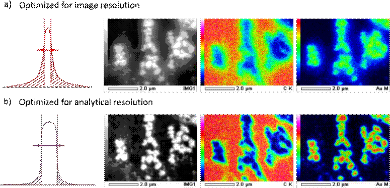
Figure 1: Beam current density on a Gaussian plane. ACL optimization at high beam currents for (a) image resolution, and (b) analytical resolution. Nano gold images and EDS analysis completed at 5 kV, 20kX, and 73 nA.
When the SEM is optimized for the smallest spot size (largest convergence angle) there is some beam tailing that produces X-rays from areas “not in the spot”. For low beam current applications this is insignificant. The best analytical data comes from the smallest convergence angle. Therefore, when the ACL is optimized for image resolution, the resulting high current image (large convergence angle) has somewhat ‘hazy’ background but shows great resolution. However, when the ACL is optimized for analytical work the ultimate resolution is slightly decreased, yet the analytical signal is no longer affected by the beam tailing resulting in smaller analytical signal delocalization (Figure 1).
The automatic optimization of the ACL maintains high resolution imaging at a wide range of accelerating voltages and probe currents, from a few picoamps to hundreds of nanoamps. This beam resolution allows very fast acquisition (using high beam current) of EDS or WDS data at low kV with high spatial resolution.
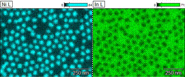
Figure 2: EDS map of nickel pillars on ITO which has sub-25nm resolution. The map was taken at 8kV with 5 nA of beam current.
Implementation of the ACL function allows collection of very fast EDS maps at high spatial resolution using low kVs. One such example is shown in Figure 2. This is an EDS map of nickel pillars on ITO with sub-25nm resolution. The map was collected at 8 kV using a beam current of 5 nA.
The ability to deliver high beam current also impacts WDS and CL (cathodoluminescence) analyses where large beam currents are needed for sufficient signal to noise collection. In the JEOL FE-SEMs, the ability of the ACL to keep the spot size small when the beam current is high results in efficient WDS mapping with high spatial resolution even at lower kV's. This is also true for CL analysis – high spatial resolution of CL collection requires a combination of high current/low voltage/small spot size.
Shown in Figure 3 is an example of slip planes in diamond imaged with panchromatic KE Centaurus CL detector at 2 kV.

Figure 3: CL image of diamond grains collected with KE Centaurus CL.